
Abstract
A 4.0λ-cavity GaN-based vertical-cavity surface-emitting laser (VCSEL) using an n-type conductive AlInN/GaN bottom distributed Bragg reflector (DBR) showed a light output power of 1.8 mW with a low differential resistance of 90 Ω. In order to obtain low resistive AlInN/GaN DBRs, 5 nm AlGaInN graded interfaces were introduced. A 40-pair AlInN/GaN DBR with the graded interfaces showed a peak reflectivity over 99.8% and a series resistance of 17 Ω. At the same time, the maximum light output power of a 1.5λ-cavity GaN-based VCSEL with the conductive DBR was only 0.03 mW due to a high thermal resistance of 2700 K W−1 caused by a high thermal resistivity of AlInN. We also conclude that a short cavity typically used in GaAs-based VCSELs is not appropriate in GaN-based VCSELs.
Export citation and abstract BibTeX RIS

Content from this work may be used under the terms of the Creative Commons Attribution 4.0 license. Any further distribution of this work must maintain attribution to the author(s) and the title of the work, journal citation and DOI.
1. Introduction
GaN-based vertical-cavity surface-emitting lasers (VCSELs) are expected to be utilized in various applications, such as retinal scanning displays, adaptive headlights, and high-speed visible light communication systems. So far, most of the GaN-based VCSELs showing room temperature (RT) continuous-wave (CW) operations have contained two dielectric distributed Bragg reflectors (DBRs)1–10) or a combination of a top dielectric DBR and a bottom undoped GaN-based DBR.10–19) Due to a lack of conductive semiconductor-based bottom DBRs, GaN-based VCSELs have required a relatively thick cavity length for double intra-cavity contacts, like 4.0λ or even thicker, leading to a low optical confinement factor. If an n-type conductive GaN-based DBR is available, like in the case of commercialized infrared GaAs-based VCSELs,20) a simple vertical current injection is possible with an electrode on the back side of the substrates. In this case, not only a high optical confinement factor but also a low differential resistance is expected by utilizing a very short (1.0 or 2.0λ) cavity length.
There are a few reports on the conductive GaN-based DBRs. Reference 21 fabricated a 26-pair n-type Al0.4Ga0.6N/GaN DBR by metalorganic vapor phase epitaxy (MOVPE), showing a peak reflectivity of 91% at 400 nm and a reasonably low differential resistance of 180 Ω in a micro cavity LED configuration. Reference 22 also reported a 20.5-pair n-type AlN/GaN grown on a SiC substrate by molecular beam epitaxy, showing a high peak reflectivity of 99% at 450 nm but a relatively high specific series resistance of 2 × 10⁻³ Ω cm2. These results imply that it is not straightforward to obtain high reflectivity and low resistivity simultaneously from the GaN-based DBRs. Under the circumstances, our group has demonstrated a RT CW operation of a 1.5λ-cavity GaN-based VCSEL with the combination of a dielectric top DBR and a 46-pair n-type conductive AlInN/GaN bottom DBR.23) The n-type AlInN/GaN DBR showed a peak reflectivity over 99.9% at 404 nm and a specific resistance of 7.8 × 10⁻⁴ Ω cm2 simultaneously by using a modulation doping of Si. While a low threshold current, 2.6 mA, was obtained, a very low light output power (LOP), a few μW, and a high differential resistance, 220 Ω, were revealed. Note that our 4.0λ-cavity GaN-based VCSELs with undoped AlInN/GaN DBR showed 3–4 mW LOPs and 120–150 Ω differential resistance.24,25) We expected a superior performance of the GaN-based VCSEL with the conductive GaN-based DBR and the short cavity, like the infrared GaAs-based VCSEL, but our previous result was not good as expected.
One of the possible reasons for the low LOP is the high differential resistance due to the DBR. In this study, we further reduced a resistance of the Si-doped n-type AlInN/GaN DBRs by introducing AlGaInN graded interfaces between AlInN and GaN, whose concept has been adopted in the commercialized infrared GaAs-based VCSELs.26) We then demonstrated GaN-based VCSELs using the optimized conductive AlInN/GaN bottom DBRs with different cavity lengths, 1.5λ and 4.0λ, and discussed the factors for the LOPs.
2. Experimental methods
In this paper, we prepared three different sets of samples grown by MOVPE. All the AlInN layers in this study were lattice-matched with GaN, containing 18% InN mole fractions. The first set of the samples was three 10-pair Si-doped AlInN/GaN DBRs with different composition profiles at the interfaces on c-plane sapphire substrates to evaluate DBR resistances under vertical current injection as shown in Fig. 1(a). The sample consisted of a 50 nm low-temperature-deposited buffer layer, a 1 μm undoped GaN layer, a 1 μm n-GaN layer with a Si concentration of 6.0 × 1018 cm−3, the 10-pair Si-doped AlInN/GaN DBR, and a 5 nm n+-GaN contact layer with a Si concentration of 1.0 × 1020 cm−3. The thicknesses of the AlInN and GaN layers were 40–45 nm, designed for a peak reflectivity wavelength of 410 nm. The growth temperatures and carrier gasses were 810 °C and nitrogen for the AlInN layers and 1020 °C and hydrogen for the GaN layers.27) Details of the different composition profiles and the modulation doping profiles of Si at the DBR interfaces are described in Fig. 1(b). The first sample contained simple abrupt interfaces at all the interfaces of the DBR. The second sample had compositionally graded AlGaInN interfaces at all the interfaces. The third sample had the graded interfaces only at the GaN/AlInN interfaces [indicated as A in Fig. 1(b)] and the abrupt interfaces at the AlInN/GaN interfaces [indicated as B in Fig. 1(b)]. In other words, the second sample had both-sided graded interfaces and the third sample had one-sided graded interfaces. Note that the graded AlGaInN interfaces were grown under 810 °C and nitrogen. A thickness of the graded interface in this study was 5 nm, which was formed by linearly changing group-III source flow rates based on the flow rates in the GaN and AlInN growth conditions. Regarding the modulation doping of Si, the highest Si concentration of 6.0 × 1019 cm−3 was doped near the GaN/AlInN interface A, and the lowest Si concentration of 5.0 × 1018 cm−3 was used near the AlInN/GaN interface B. After the DBR epitaxial growth, a 35 μm diameter mesa was formed by dry etching, and Cr/Ni/Au electrodes were deposited on the top of the mesa and on the etched surface of the n-GaN layer.
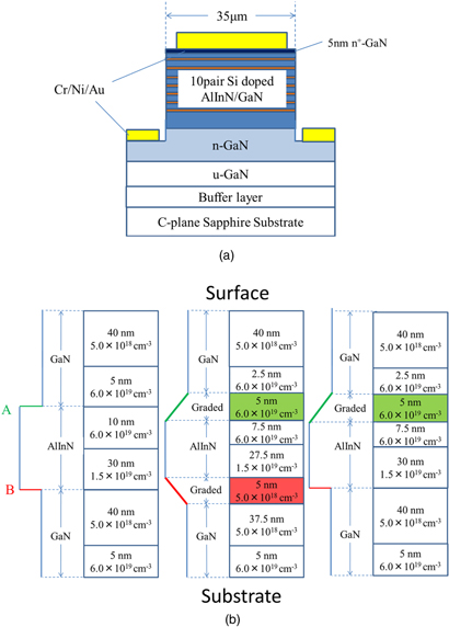
Fig. 1. (Color online) (a) Schematics of a 10-pair Si-doped AlInN/GaN DBR structure for I–V measurement, and (b) layer structures and Si doping profiles in GaN/AlInN/GaN.
Download figure:
Standard image High-resolution imageWe also calculated energy profiles of conduction band minima in the first (with abrupt interfaces) and second (with graded interfaces) samples. In general, the abrupt interfaces between two semiconductors with different band gaps form energy spikes, suppressing smooth carrier transport. Here not only the modulation doping profiles of Si but also the spontaneous polarization charges (±2.7 × 1013 cm−2)28) at the interfaces were considered in the calculation.
The second set of samples was two 40-pair AlInN/GaN DBRs grown on GaN substrates for reflectivity measurements. One sample was a 40-pair Si-doped AlInN/GaN DBRs with the one-sided graded interfaces identical to those of the third sample in the first set, but without the n+-GaN contact layer for surface morphology and reflectivity measurements. The other was a 40-pair undoped abrupt AlInN/GaN DBR for comparison. After the reflectivity measurements, the 5 nm n+-GaN layer was grown on the 40-pair Si-doped DBR for a vertical resistance measurement. As shown in Fig. 2, a 25 μm diameter Cr/Ni/Au electrode was deposited on the n+-GaN contact layer without any mesa etching. The other electrode was also deposited on the back side of the substrate. Note that a current distribution in this structure without mesa etching could be close to that in the actual VCSEL.
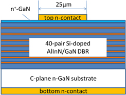
Fig. 2. (Color online) A schematic of a 40-pair Si-doped AlInN/GaN DBR structure for I–V measurement.
Download figure:
Standard image High-resolution imageThe third set of samples was two GaN-based VCSELs with the 40-pair Si-doped AlInN/GaN bottom DBRs with different cavity lengths of 1.5λ and 4.0λ on GaN substrates, as shown in Fig. 3. The VCSEL structure contains the 40-pair Si-doped AlInN/GaN DBR with the one-sided graded interfaces, a 50 nm (1.5λ) or 450 nm (4.0λ) n-GaN, 3 nm GaInN/6 nm GaN five quantum wells emitting around 405 nm wavelength, a 20 nm p-Al0.2Ga0.8N electron blocking layer, a 60 nm p-GaN, and a 10 nm p+-GaN contact layer. After the MOVPE growth of all the above-mentioned layers, a 40 μm diameter mesa was formed by dry etching. A combination of an 8 μm diameter aperture of SiO2 layer and an ITO electrode for current confinement was formed on the mesa. Then, a top ring electrode was deposited on the peripheral area of the ITO electrode. A Nb2O5 spacer layer and an 8-pair Nb2O5/SiO2 top DBR, showing a 99.9% reflectivity, were also deposited on the center of ITO electrode. Finally, a bottom electrode was deposited on the back side of the GaN substrates.
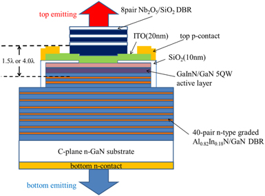
Fig. 3. (Color online) A schematic of a GaN-based VCSEL with vertical current injection through the n-type conductive AlInN/GaN DBR.
Download figure:
Standard image High-resolution imageWe performed the following measurements for the samples. Current–voltage (I–V) characteristics under vertical current injection through the DBR were measured with the samples in the first and second sets. Surface morphology of samples in the second set were measured by atomic force microscopy (AFM). Reflectivity spectra of the samples in the second set were measured by an absolute reflectivity measurement system. Current–voltage–LOP (I–V–L) characteristics of the samples in the third set were measured under RT CW conditions.
3. Results and discussion
Figure 4 shows I–V characteristics of the 10-pair Si-doped AlInN/GaN DBR with the various composition profiles at the interfaces. While the sample with the abrupt interfaces showed Schottky behavior, the samples with the both-sided and one-sided graded interfaces showed ohmic behavior, resulting in the same low resistances. The resistance values were 18 Ω, including a lateral resistance of the n-GaN as shown in Fig. 1(a). This result clearly suggests that a drastic resistance reduction came from the graded layers at the interfaces of GaN on AlInN [indicated as A in Fig. 1(b)] but not those at the interfaces of AlInN on GaN [indicated as B in Fig. 1(b)]. Actually, the calculated energy profiles of the conduction band minima predicted the above results. As shown in Fig. 5, the sharp energy spikes were formed only in the sample with the abrupt interfaces. An interesting point is that the energy spike at the abrupt AlInN/GaN interface (indicated as B in Fig. 5) was formed only toward the lower direction, which did not interfere the electron transport in the conduction band. This is because the positive polarization charges at the AlInN/GaN interface originally pull down the conduction band minima, resulting in the accumulation of a large number of electrons there to satisfy the charge neutrality condition. On the contrary, the large energy spike at the abrupt GaN/AlInN interface (indicated as A in Fig. 5) seems to suppress smooth electron transport, leading to the Schottky behavior observed in Fig. 4. Then the graded layer at the interface is very effective to eliminate the energy spike, contributing a lot to the low resistance shown in Fig. 4. As a result, the one-sided graded interfaces at the negative polarization charges (e.g. GaN/AlInN) with the Si concentration of 6.0 × 1019 cm−3 are sufficient to obtain low resistance of AlInN/GaN DBRs.
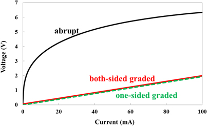
Fig. 4. (Color online) I–V characteristics of 10-pair AlInN/GaN DBRs with the abrupt interfaces, the both-sided graded interfaces, and the one-sided graded interfaces.
Download figure:
Standard image High-resolution image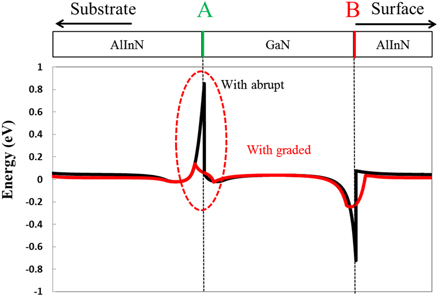
Fig. 5. (Color online) Calculated band profiles of GaN/AlInN/GaN with and without graded interfaces.
Download figure:
Standard image High-resolution imageFigure 6 shows surface morphologies of (a) the 40-pair Si-doped AlInN/GaN DBRs with the one-sided graded interfaces and (b) the 40-pair undoped AlInN/GaN DBR with the abrupt interfaces. The surface morphologies of both the DBRs were very smooth with less than 0.1 nm of RMS values in the AFM images, suggesting that adverse effects of the Si doping were small.
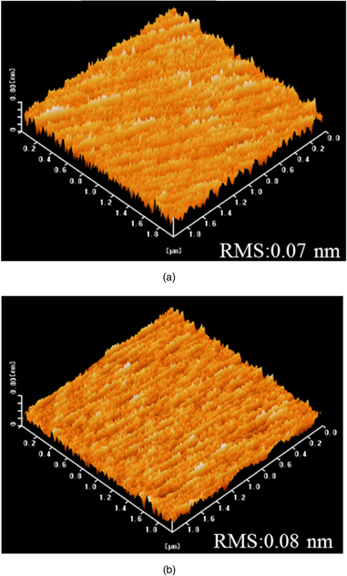
Fig. 6 (Color online) 2 × 2 μm2 AFM images of (a) a 40-pair Si-doped AlInN/GaN DBR with the one-sided graded interfaces and (b) a 40-pair undoped AlInN/GaN DBR.
Download figure:
Standard image High-resolution imageFigures 7(a) and 7(b) show wide-range and narrow-range reflectivity spectra of the 40-pair Si-doped AlInN/GaN DBRs with the one-sided graded interfaces and the 40-pair undoped AlInN/GaN DBR with the abrupt interfaces. The stop bands with about 22 nm widths above a 90% reflectivity and many clear side lobes were consistently observed from both the DBRs in Fig. 7(a). Then, the 40-pair Si-doped graded AlInN/GaN DBR showed a peak reflectivity over 99.8% at 408 nm estimated from an averaged line, which was very close to that (99.9% at 413 nm) of the 40-pair undoped AlInN/GaN DBR in Fig. 7(b). Note that the two DBRs were grown at different dates. The wavelength shift (about 1%) in stop band between the undoped DBR and the Si-doped graded DBR should be caused by a slight difference in the DBR growth rates.
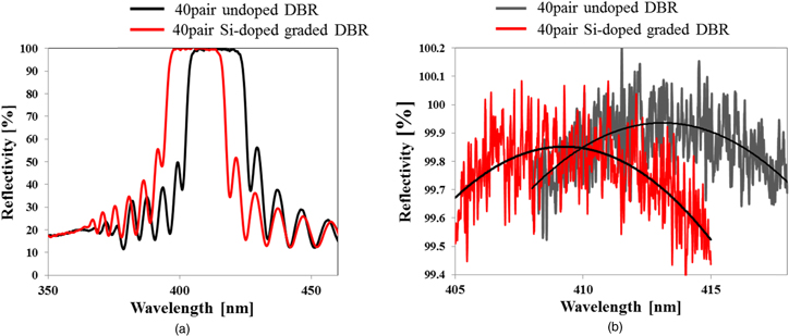
Fig. 7. (Color online) (a) Wide-range and (b) narrow-range spectra of a 40-pair Si-doped AlInN/GaN DBR with the one-sided graded interfaces and a 40-pair undoped AlInN/GaN DBR.
Download figure:
Standard image High-resolution imageThe I–V characteristics of the 40-pair Si-doped AlInN/GaN DBR with the regrown n+-GaN contact layer under vertical current injection from the wafer surface to the back side of the GaN substrate are shown in Fig. 8. A series resistance was 17 Ω, which seems reasonably low compared to differential resistance values of our VCSELs described above. We conclude that our 40-pair Si-doped AlInN/GaN DBR with one-sided graded layers shows sufficiently high reflectivity and reasonably low resistance simultaneously.
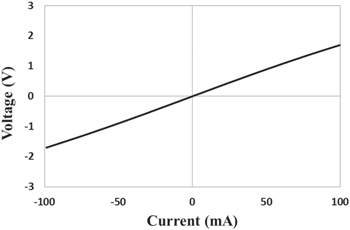
Fig. 8. (Color online) I–V characteristics under a vertical current injection through the 40-pair Si-doped AlInN/GaN DBR with the one-sided graded interfaces.
Download figure:
Standard image High-resolution imageFigure 9 shows I–V–L characteristics of the 1.5λ-cavity and 4.0λ-cavity GaN-based VCSELs with the 40-pair Si-doped AlInN/GaN bottom DBRs containing one-sided graded interfaces under RT CW operation. Note that here LOP values were measured from the top dielectric DBRs, meaning that the LOPs should be lower than those from the bottom AlInN/GaN DBRs because of the higher reflectivity. As shown in Fig. 9, we obtained low differential resistances of 90–95 Ω from both the VCSELs. The differential resistance was largely decreased by introducing the vertical current injection with the Si-doped AlInN/GaN bottom DBR with the one-sided graded interfaces at the GaN/AlInN. While a threshold current of 7.0 mA (14 kA cm−2 as a threshold current density) was obtained from the 4.0λ-cavity VCSEL, 3.1 mA (6.2 kA cm−2) was obtained from the 1.5λ-cavity VCSEL. Such a reduction of the threshold current density of the 1.5λ-cavity VCSEL could be due to the larger optical confinement factor from the short cavity and/or a small detuning described later. At the same time, the maximum LOP of the 1.5λ-cavity VCSEL was only 0.03 mW obtained at 5.3 mA, while that of the 4.0λ-cavity VCSEL was 0.45 mW at 15 mA.
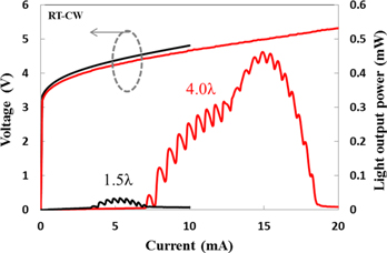
Fig. 9. (Color online) I–V–L characteristics of the 1.5λ-cavity and 4.0λ-cavity GaN-based VCSELs with the 40-pair n-type conductive AlInN/GaN bottom DBR. The LOPs were measured from the top DBRs.
Download figure:
Standard image High-resolution imageConsidering the difference in current at rollover point between the two VCSELs (5.3 mA versus 15 mA), thermal resistances were estimated by measuring input power and environment temperature dependences on resonance wavelengths of the VCSELs. Figures 10(a) and 10(b) show the resonance wavelengths as a function of input power and environment temperature. Slopes of wavelength to input power (Δλ/ΔP) and those of wavelength to environment temperature (Δλ/ΔT) were estimated to be 42.1 nm W−1 and 0.0156 nm °C−1 for the 1.5λ-cavity VCSEL, and 21.5 nm W−1 and 0.0161 nm °C−1 for the 4λ-cavity VCSEL, respectively. Then the thermal resistance, Rth, is estimated by Eq. (1)

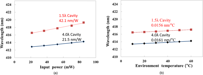
Fig. 10. (Color online) (a) Input power and (b) environment temperature dependences on resonance wavelengths of the GaN-based VCSELs under CW operations.
Download figure:
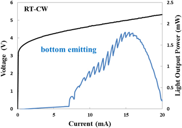
Standard image High-resolution imageThe Rth values were estimated to be 2700 K W−1 for the 1.5λ-cavity VCSEL and 1340 K W−1 for the 4.0λ-cavity VCSEL. A double Rth value from the 1.5λ-cavity VCSEL came from a double Δλ/ΔP value compared to those of the 4.0λ-cavity VCSEL as shown in Fig. 10(a). Recently Ref. 29 reported the thermal resistances of the 5.0λ-cavity and 10λ-cavity VCSELs with p-side down bonding to Cu heat sink. Their values of the 5.0λ-cavity and 10λ-cavity VCSELs were 0.0142 and 0.0146 nm C−1 of Δλ/ΔT and 15.0 and 10.3 nm W−1 of Δλ/ΔP, respectively. While the Δλ/ΔT values are very similar (0.014–0.016 nm °C−1), our Δλ/ΔP values also seem to have the same cavity thickness dependence as Ref. 30 suggested. The poor thermal characteristics of the short cavity GaN-based VCSELs, which is unlike the GaAs-based VCSEL, is attributed to a very high thermal resistivity of AlInN. We then estimated that device temperatures at the rollover points were 73 °C for the 1.5λ-cavity VCSEL and 98 °C for the 4.0λ-cavity VCSEL. The difference of the two device temperatures at the rollover points could be due to a different detuning between gain peak wavelength and the resonance wavelength, and the detuning could be smaller in the 1.5λ-cavity VCSEL as described above. After all, we must conclude that the short cavity with the conductive DBR which is useful for infrared GaAs-based VCSELs is not appropriate for visible GaN-based VCSELs with the AlInN/GaN bottom DBR. Finally we measured the LOP of the 4.0λ-cavity GaN-based VCSEL with the Si-doped conductive AlInN/GaN DBR from the bottom DBR with a lower reflectivity. As shown in Fig. 11, the maximum LOP was 1.8 mW, and a differential external quantum efficiency was 7.5%. Even though we demonstrated a mW-class GaN-based VCSEL with the Si-doped conductive DBR, this value was lower than that of our 4.0λ-cavity VCSEL with undoped DBR (3–4 mW).24,25) At the same time, as shown in Figs. 6 and 7, the Si-doped conductive DBR showed a similar quality as the undopoed DBR. Thus, the lower LOP could be not the DBR quality but a layer thickness adjustment typically required for the VCSEL cavity.
Fig. 11. (Color online) I–V–L characteristics of the 4.0λ-cavity GaN-based VCSEL with the n-type conductive AlInN/GaN DBR. The LOP was measured from the bottom DBR.
Download figure:
Standard image High-resolution image
4. Conclusions
In summary, the n-type conductive AlInN/GaN DBRs were optimized by introducing the graded interfaces in the DBRs. The one-sided graded interfaces with the high Si concentrations at the negative polarization charges are very effective to obtain the AlInN/GaN DBR showing the peak reflectivity over 99.8% and the series resistance of 17 Ω. We then demonstrated RT CW operations of the 1.5λ and 4.0λ-cavity GaN-based VCSELs with the n-type conductive AlInN/GaN DBRs, showing low differential resistances of 90–95 Ω. We found that the maximum LOP of the 1.5λ-cavity VCSEL was only 0.03 mW. This is because the 1.5λ-cavity contains the high thermal resistance of 2700 K W−1 due to the high thermal resistivity of AlInN in the bottom DBR. In contrast, the 4.0λ-cavity GaN-based VCSEL showed a LOP of 1.8 mW. We conclude that the short cavity is not appropriate for visible GaN-based VCSELs with AlInN/GaN DBR.
Acknowledgments
This work was partially supported by the MEXT Private University Research Branding Project (2016–2020), the JSPS KAKENHI for Scientific Research A (15H02019), the JSPS KAKENHI for Scientific Research A (17H01055), and the JSPS KAKENHI for Innovative Areas (16H06416).